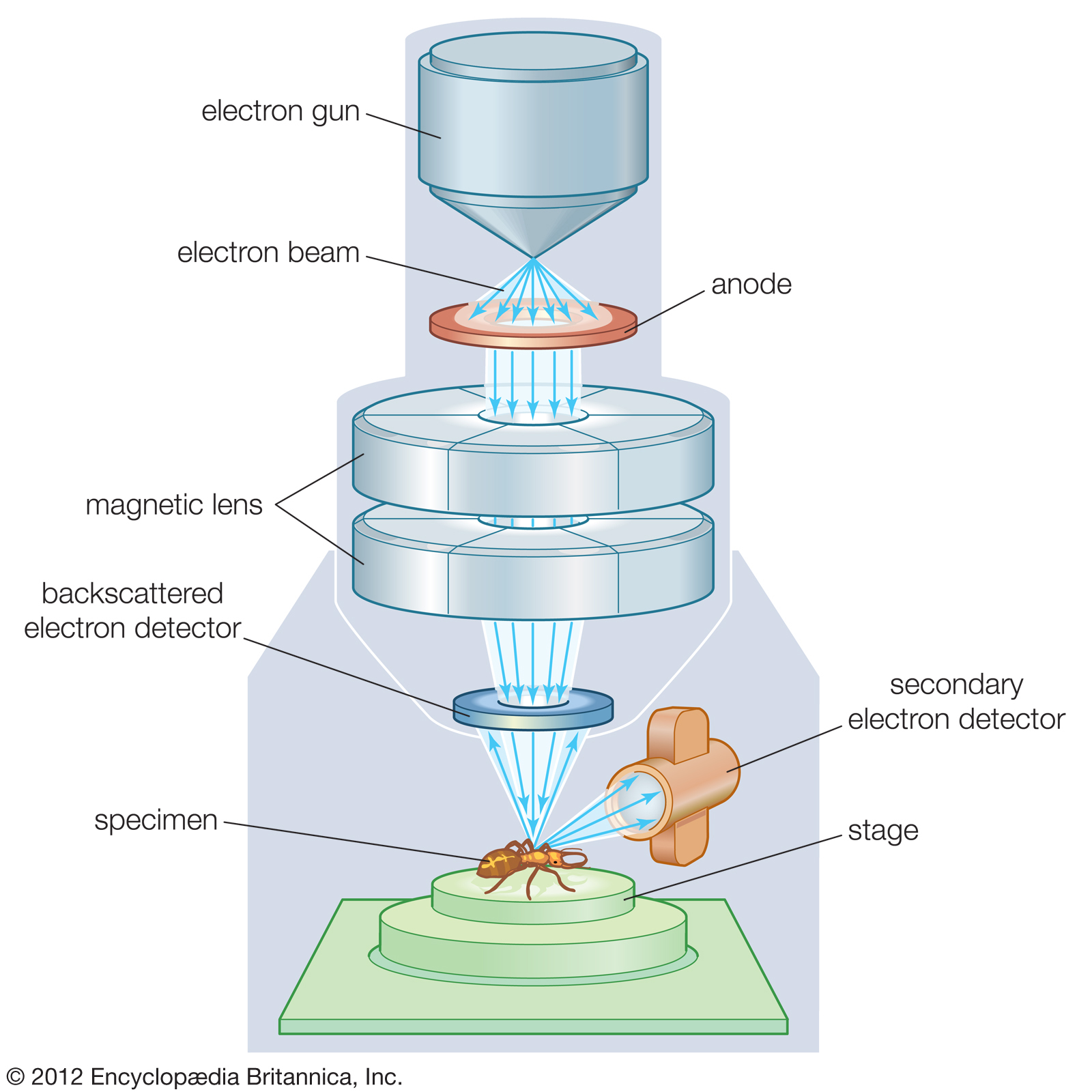
In scanning electron microscopy (SEM), a beam of electrons scans the surface of a specimen, providing detailed, magnified images.
This is different to optical microscopy, which involves viewing objects through a magnified lens using visible light.
Electron microscopy has certain advantages over optical microscopy.
How Do Electron Microscopes Work?
Using electron beams, an electron microscope can give a very high quality of imaging, as an advanced means of sample analysis.
In SEM, an electron gun fires an electron beam which is focussed through a series of lenses and apertures on the microscope.
When these beams hit the sample, they interact with atoms on its surface, emitting secondary electrons, backscattered electrons, and x-rays.
The microscope has built-in detectors that pick up these signals, using them to create high-resolution images and provide information on the composition of the specimen.
The SEM operates under vacuum conditions, which prevents atoms or molecules interacting with the electrons, and therefore ensures a high quality of imaging.
What are the Uses of Electron Microscopy?
SEM has a broad range of research applications, and is a highly practical method for obtaining information on the surface topography and composition of a specimen.
- Composition – what a sample is made up of
Secondary electrons (SE) are emitted when the elctrom beam excites electrons in the sample. There is a loss of energy (inelastic interaction) and the low energy secondary electrons and can only escape from the outer few nanometers of the sample, making them useful for imaging surface topography.
Alternatively high energy electrons in the electron beam can effectively bounce off the sample with essentially no energy loss (elastic scattering). These back scattered electrons (BSE) can escape larger area of the sample, so have lower topographical resolution than SE. The amount of BSE emitted, however, increases with increasing atomic mass in the specimen. This provides compositional imaging as heavier elements appear brighter.
The electron beam also causes atoms to emit x-rays, with energies specific to the elements that are present. These can be used to identify and quantify the elements in the specimen, and create an image (or map) of the element distribution.This is called Energy Dispersive spectrometry (EDS)
Various sectors and industries use SEM.
In biological sciences, it is used to test vaccines and identify bacterial strains, and it is used in genetics. It can help uncover new species of organisms, or to monitor the effect of environmental changes on existing organisms.
Medical science uses SEM for comparing blood and tissue samples, identifying viruses and diseases and testing new medicines.
In the field of forensics, SEM can analyse fibres and other particles at crime scenes, and analyse gunshot residue. It is also an effective method for close analysis of handwriting and print. It can detect forged banknotes, for example.
In electronics, SEM helps with microchip assembly involving progressively smaller components and materials. It is useful for inspecting and testing semiconductors and in other areas of quality control.
Various areas and disciplines of materials science use SEM for research, and SEM is an ideal tool for microscopic levels of quality control.
SEM is used extensively in geology to study rocks, minerals, and (micro) fossils and is therefore appied in the mining and oil industries.
Advantages of Electron Microscopy over Optical Microscopy
The naked human eye should be able to distinguish between two points of light 0.2mm apart, given good lighting conditions. This distance is the eye’s resolution.
If you use an optical microscope, you can magnify this resolution, which enables the eye to see points that are closer together than 0.2mm.
An optical microscope will have a maximum magnification power of between 500x and 1500x.
This is considerably lower than an electron microscope, which can have a maximum magnification of around 160,000x.
A limiting factor in optical microscopes, which use light for magnification, is wavelength. The wavelengths of white light are between 400 and 700nm (nanometers), and the average is 500nm.
This gives optical microscopes a resolution detection limit somewhere between 200 and 250nm.
But electron microscopes use shorter wavelengths, which give better image resolution. Some can achieve resolutions below 1nm.
A typical full-sized instrument produces resolutions between 1 and 20nm, while a smaller desktop model will produce resolutions of 20nm and over.
Another advantage a scanning electron microscopes has over an optical microscope is the capability to view the three-dimensional structures of objects. and have greater depth of field.
Electron microscopes can also provide information on the composition of the sample.
Which Type of Microscope Should You Use?
Due to the advantages we have outlined, electron microscopes are ideal for a range of applications. However, for certain purposes, such as observing living cells, optical microscopes are essential.
Essentially, the two types of microscope complement, rather than compete against, one another.
What you do get with electron microscopes is the capability of extremely high magnification and image resolution, excellent surface viewing, and compositional information.